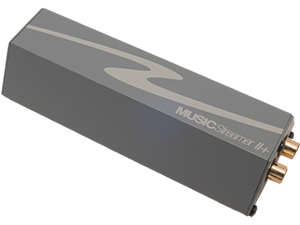
Detet ligger på Audiofreaks.no sin forside nå. Tydligvis skrevet av HRT Kevin Halverson:
Jitter:
This is a complex subject; specifically that the measurement of jitter, via analysis of an analogue output, is not a trivial task and one that is frequently done incorrectly in many, if not most, audio publications.
In order to declare an artifact that is present in an analogue output from a converter as having been caused by clock jitter, is difficult, as there are many potential contributors, only some of which might be the result of jitter, and many of which can not be reliably correlated.
The often used and wholly wrong approach of using a bi-phase excitation signal for non bi-phase interfaces, leads to clear errors of distinction. The bi-phase excitation approach toggles the LSB, and since the bi-phase interface uses a two's complement data stream, the result is a large change in the resulting data. Bi-phase clock recovery circuits are severely affected by this type of event and exhibit markers of considerable magnitude, which can be used to quantify their ability to reject jitter (correctly expressed as jitter rejection often in units of dB's).
When one considers interface jitter in, for example, a USB connected device, there are other mechanism in play, and depending upon the interface type, will have different spectra. Consider the adaptive interface as an example. In this approach, only the SOF (Start of Frame) events can be used by the device (as opposed to the host) to extract an upstream clock. In the case of a FS (Full Speed) USB interface, these are 1 ms events. In the case of a HS (High Speed) USB interface these are 125 us (microsecond) events. Since the data packet which is delineated by the SOF (and EOF as well) event can occur anywhere within the slot, one can see that there is a clear mechanism for interface jitter which is centered around either 1 or 8 kHz, and has a bandwidth bounded by the delta t (which can be calculated, but is beyond what one has time to explain in this brief document). If one knew what interface methodology was employed, one could then speculate that certain analog audio components were contributed by clock jitter which resulted from interface jitter. However, the appropriate excitation would not be one which is designed to excite bi-phase interfaces and the analysis parameters would be different as the resulting spectra would also be different. This is equally true of say for example, single box players where no bi-phase interface is present.
There are numerous mechanisms which can generate output artifacts; their analysis is not a trivial task, and one that can not be performed properly on a 'closed box or DUT' (Device Under Test) approach, without some very specific knowledge of the characteristics of the device. One could list an almost infinite number of sources, so let's just illustrate a few.
Consider that a digital gate is essentially a high gain analog comparator (either open loop or with de or regenerative feedback depending upon the desired characteristics, an example of which would be a schmitt trigger logic family device) and that any noise conducted will have an effect on its logic threshold and since all applied signals have finite bandwidth (greater than zero rise/fall times) the change in threshold will shift in time the point when a logic state changes. The mechanism for noise to be coupled can be via either the power or ground bus and can be directly conducted into or induced into either the logic or power/ground terminals). This source of this timing error is correctly described as jitter but its contributors are most certainly outside of the characteristics of the interface. All sources of noise can and will almost certainly contribute to a modulation of the event threshold.
In the case of a locally clocked device (an example of which would be an asynchronous transfer protocol USB interface) can be effected by the phase noise of the local clock, noise induced from any number of sources (including local processing) and numerous other events.Another area worthy of consideration, is the effect different forms of clock jitter have on different conversion topologies. In the case of so called 'ladder DACs' they are somewhat easier to understand, but in noise shaped delta sigma types, the complexity quickly becomes considerable.
One could go on for pages describing potential contributors and approaches which either exacerbate or mitigate their effect, but this is again beyond the scope of this missive. The point is that attribution of a spectral plot has to be carefully considered, and to have any hope of accuracy, the excitation should be designed to provide a marker (such as the what the bi-phase test does with a bi-phase interface).
Presuming that one understands these points, the next logical step is to call into question most of what has been published over the years. Certainly some of what has been measured can be described accurately as jitter, but much can only be speculation. If you look at some of the work done in this area, an example of which is Paul Miller's analysis solution, did attempt to label some markers with their likely causes, and many others which were of an undefined origin.
The proper measurement of jitter is made when looking at a clock directly. Only then can one accurately declare the characteristics of the delta t via either a peak to peak measurement or via a more elaborate binning and spectral distribution model.
Jitter measurement can only be made when looking at a clock, and that looking at an analogue signal is clearly not measuring jitter- at best it is measuring an artifact which 'might' be caused by clock jitter.
Audiophiles often have the desire to latch upon a bit of knowledge and a desire to have a numeric value that they can use to make a pseudo objective comparison. The general misunderstanding of jitter in general, and the contribution that it can have to mode conversion (ADC or DAC) device has not been helped by the poor quality of information disseminated over the years.
")